- 您现在的位置:买卖IC网 > Sheet目录3753 > ATMEGA169P-16MCHR (Atmel)MCU AVR 16KB FLASH 16MHZ 64-VQFN
PIC16F946
DS41265A-page 152
Preliminary
2005 Microchip Technology Inc.
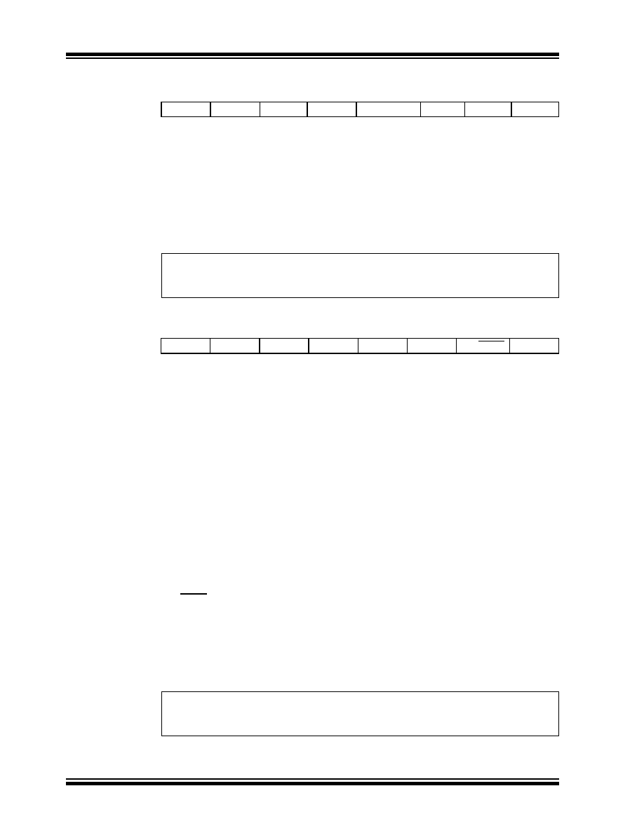
REGISTER 12-1:
ANSEL – ANALOG SELECT REGISTER (ADDRESS: 91h)
REGISTER 12-2:
ADCON0 – A/D CONTROL REGISTER (ADDRESS: 1Fh)
R/W-1
ANS7
ANS6
ANS5
ANS4
ANS3
ANS2
ANS1
ANS0
bit 7
bit 0
bit 7-0:
ANS<7:0>: Analog Select bits
Select between analog or digital function on pins AN<7:0>, respectively.
1
= Analog input. Pin is assigned as analog input.(1)
0
= Digital I/O. Pin is assigned to port or special function.
Note 1: Setting a pin to an analog input automatically disables the digital input circuitry,
weak pull-ups, and interrupt-on-change, if available. The corresponding TRIS bit
must be set to Input mode in order to allow external control of the voltage on the pin.
Legend:
R = Readable bit
W = Writable bit
U = Unimplemented bit, read as ‘0’
- n = Value at POR
‘1’ = Bit is set
‘0’ = Bit is cleared
x = Bit is unknown
R/W-0
ADFM
VCFG1
VCFG0
CHS2
CHS1
CHS0
GO/DONE
ADON
bit 7
bit 0
bit 7
ADFM: A/D Result Formed Select bit
1
= Right justified
0
= Left justified
bit 6
VCFG1: Voltage Reference bit
1
= VREF- pin
0
= VSS
bit 5
VCFG0: Voltage Reference bit
1
= VREF+ pin
0
= VDD
bit 4-2
CHS<2:0>: Analog Channel Select bits
000
= Channel 00 (AN0)
001
= Channel 01 (AN1)
010
= Channel 02 (AN2)
011
= Channel 03 (AN3)
100
= Channel 04 (AN4)
101
= Channel 05 (AN5)
110
= Channel 06 (AN6)
111
= Channel 07 (AN7)
bit 1
GO/DONE: A/D Conversion Status bit
1
= A/D conversion cycle in progress. Setting this bit starts an A/D conversion cycle.
This bit is automatically cleared by hardware when the A/D conversion has completed.
0
= A/D conversion completed/not in progress
bit 0
ADON: A/D Conversion Status bit
1
= A/D converter module is operating
0
= A/D converter is shut off and consumes no operating current
Legend:
R = Readable bit
W = Writable bit
U = Unimplemented bit, read as ‘0’
- n = Value at POR
‘1’ = Bit is set
‘0’ = Bit is cleared
x = Bit is unknown
发布紧急采购,3分钟左右您将得到回复。
相关PDF资料
2-1546217-0
TERM BLK RCPT 20POS SIDE 5.08MM
1-1546217-9
TERM BLK RCPT 19POS SIDE 5.08MM
1-1546217-8
TERM BLK RCPT 18POS SIDE 5.08MM
1-1546217-7
TERM BLK RCPT 17POS SIDE 5.08MM
1-1546217-6
TERM BLK RCPT 16POS SIDE 5.08MM
1-1546217-5
TERM BLK RCPT 15POS SIDE 5.08MM
1-1546217-4
TERM BLK RCPT 14POS SIDE 5.08MM
1-1546217-3
TERM BLK RCPT 13POS SIDE 5.08MM
相关代理商/技术参数
ATMEGA169P-16MCU
功能描述:8位微控制器 -MCU AVR 16KB, 512B EE 16MHz 1KB SRAM, 5V
RoHS:否 制造商:Silicon Labs 核心:8051 处理器系列:C8051F39x 数据总线宽度:8 bit 最大时钟频率:50 MHz 程序存储器大小:16 KB 数据 RAM 大小:1 KB 片上 ADC:Yes 工作电源电压:1.8 V to 3.6 V 工作温度范围:- 40 C to + 105 C 封装 / 箱体:QFN-20 安装风格:SMD/SMT
ATMEGA169P-16MU
功能描述:8位微控制器 -MCU AVR 16K FLASH 512B EE 1K SRAM LCD ADC RoHS:否 制造商:Silicon Labs 核心:8051 处理器系列:C8051F39x 数据总线宽度:8 bit 最大时钟频率:50 MHz 程序存储器大小:16 KB 数据 RAM 大小:1 KB 片上 ADC:Yes 工作电源电压:1.8 V to 3.6 V 工作温度范围:- 40 C to + 105 C 封装 / 箱体:QFN-20 安装风格:SMD/SMT
ATMEGA169P-16MU SL383
制造商:Atmel Corporation 功能描述:MCU 8BIT ATMEGA RISC 16KB FLASH 3.3V/5V 64PIN MLF - Tape and Reel
ATMEGA169P-16MUR
功能描述:8位微控制器 -MCU AVR LCD 16KB FLSH EE 512B 1KB SRAM-16MHZ RoHS:否 制造商:Silicon Labs 核心:8051 处理器系列:C8051F39x 数据总线宽度:8 bit 最大时钟频率:50 MHz 程序存储器大小:16 KB 数据 RAM 大小:1 KB 片上 ADC:Yes 工作电源电压:1.8 V to 3.6 V 工作温度范围:- 40 C to + 105 C 封装 / 箱体:QFN-20 安装风格:SMD/SMT
ATMEGA169P-8AU
制造商:ATMEL 制造商全称:ATMEL Corporation 功能描述:Microcontroller with 16K Bytes In-System Programmable Flash
ATMEGA169P-8MU
制造商:ATMEL 制造商全称:ATMEL Corporation 功能描述:Microcontroller with 16K Bytes In-System Programmable Flash
ATMEGA169PA
制造商:ATMEL 制造商全称:ATMEL Corporation 功能描述:8-bit Microcontroller with 16K Bytes In-System Programmable Flash
ATMEGA169PA_1
制造商:ATMEL 制造商全称:ATMEL Corporation 功能描述:High Endurance Non-volatile Memory segments